
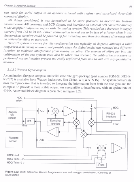
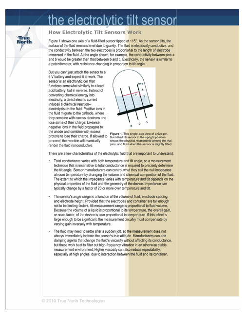
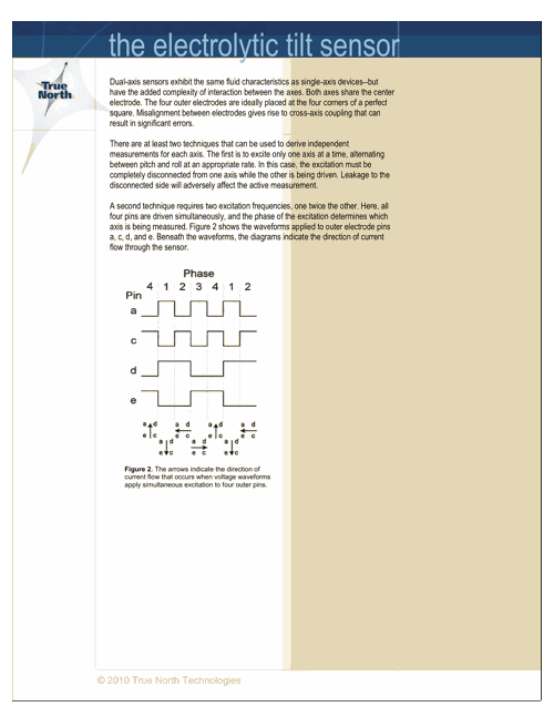
VFX1 Linkbox Theory of Operation
By Kevin Mellott
Table of
Contents
1.
VFX1 System overview
2.
VFX1 Video
2.1 Operation
2.2 Composite
Video
2.3 RGB
2.4 Stereo 3D
3.
VFX1 Head
tracking and Cyberpuck
3.1 Communication protocol
3.1.1 ACCESS.bus
3.1.2 Data Stream
and Timing
3.2 Sensor Operation
3.2.1 Fluxgate
3.2.2 Electrolytic
Tilt Sensor
3.3 Tracking Linkbox
4.
Full Linkbox Solution
5.
Calibration
Suite
5.1 Calibration Tilt Table
5.2 Electrolytic Tilt Sensor Calibration
5.3 Fluxgate Calibration
5.4 Generating a Heading
5.5 Mouse Code
1.
System Overview
The original VFX1 system consisted of the VFX1 HMD, Cyberpuck, and a VIP card. The VIP card plugged into an ISA slot in the PC and handled all the communication between the PC and the VFX1/Cyberpuck. Figure 1 below shows an image of the original VFX1 system.
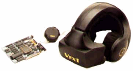
Figure 1: VFX1 System
The reason for this document is to explain the operation of the VFX1 and the creation of a linkbox that allows the VFX1 to be connected to current generation computers and laptops. A system block diagram of the VFX1 system is shown below in Figure 2.
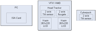
Figure 2: Block diagram of VFX1 System
Reverse engineering of the head tracker, video system, and communication bus are needed to operate the VFX1 HMD without the need of the VIP card. The Cyberpuck internals are a subset of the VFX1 head tracker, containing just a microcontroller and a 2-axis tilt sensor.
The operation of the VFX1 LCDs and head tracking will be discussed below along with Cyberpuck operation.
2.
VFX1 Video
The backlit LCDs in the VFX1 are Kopin 789 x 230 microdisplays which gave a color resolution of 263(3) x 230. The incoming video is processed by a Sharp IR3Y15 video processing chip which can take Composite video input or RGB. The Sharp video IC can also run NTSC or PAL for the composite video. Sharp denies this chip was ever produced but a close cousin the IR3Y05 was used in the CyberMaxx HMD as well. The Kopin LCDs themselves are driven by a ETM3070 timing chip.
2.2
Composite Video
The IR3Y15 datasheet, and the schematic shown below in Figure 3 for the Cybermaxx HMD, have been used to modify the VFX1 to accept composite video input instead of RGB.
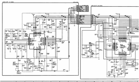
Figure 3: Cybermaxx HMD Schematic with IR3Y05
Sharp IC
The LCD boards in the VFX1 HMD contain all the footprints to place parts for NTSC or PAL composite video operation. The parts just haven’t been loaded.
A hand drawn schematic of the VFX1 LCD board setup for NTSC composite video input is shown below in Figure 4.
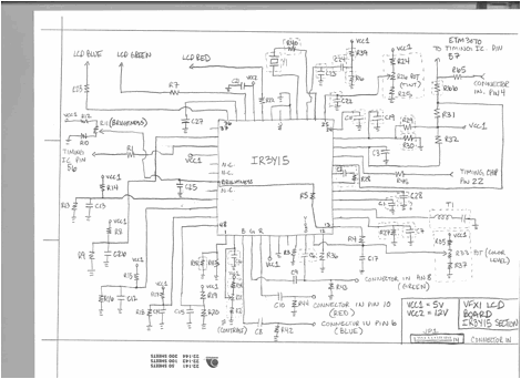
Figure 4: Composite Video
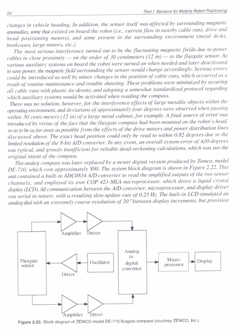
LCD Schematic
2.3
RGB
RGB video is the default video format of the VFX1. The RGB video is run at a Television horizontal scan rate of 15.75kHz with vertical scan rate of 60Hz. This is HALF the frequency of the 31.5kHz horizontal scan frequency of a typical VGA signal. What occurs is a double image in both LCDs if you attempt to feed it a VGA signal. This was the discussion of many many people early on trying to develop a video linkbox for the VFX1 system.
In order to display video on the VFX1 a SCART output of a video scan converter is needed. This outputs RGB at the correct frequencies. Some video converters will call this the “RGB” output. The converter that has been used in this linkbox solution is the PC/TV Genie (Fig. 5) by Averlogic. This converter was a way for them to demo and show off their AL128 video logic chip.
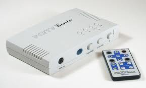
Figure 5: PC/TV Genie
Two PC/TV genies are needed if you want to run stereo 3D. Otherwise a single converter can be used to drive both left and right video lines. There is one modification that is needed. The Csync line must be inverted for the VFX1 to behave properly.
The first video linkboxes developed used a single PC/TV Genie with inverter and power supply. A pinout of the VFX1 DB26 connector and the connections to the PC/TV SCART output are shown below in Figure 6.
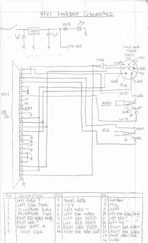
Figure 6: VFX1 DB26 to
PC/TV Genie SCART Output Schematic
In Figure 6 above the schematic is shown for the first video linkbox that was developed. The original hardware is shown below in Figure 7. In this arrangement the VFX1 LCD backlights were hard wired on because there was no interface to the ACCESS.bus interface of the HMD.
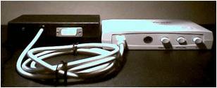
Figure 7: First Video Linkbox for the VFX1 HMD
2.4
Stereo 3D
Rob Smith at the yahoo groups fortevr group originally posted the schematic below to introduce line blanking stereo 3D on the VFX1 without the use of the VIP card.
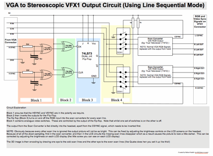
Figure 8: Rob Smith’s Line Blanking Stereo 3D Schematic
This schematic has been successfully adapted using PC/TV Genies for stereo 3D and used to play Quake in original 3D mode. The eagleCad schematics for the stereo 3D switcher is shown below in Figures 9 and 10. One modification that needs to be done is that the RC circuits on the inputs don’t always output a logic level that’s in a defined logic region for TTL circuits. Comparators need to be put on the outputs of the RC circuits so that they’re always a defined logic level of 1 or 0. This was the only issue found in using Rob Smith’s schematic.
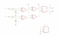
Figure 9: Video Switcher Schematic #1
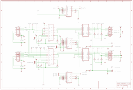
Figure 10: Video Switcher Schematic #2
In Figures 9 and 10 above, the board is actually setup to take dual VGA inputs for stereo as well. Most likely this will be dropped in the future for just the simplistic line-blanking stereo 3D mode.
This schematic feeds left and right images to the seperate PC/TV Genies. Every other video line is routed to the appropriate output via the video switches. This switching is triggered on horizontal sync pulses and reset at the end of a frame by the vertical sync pulse. The only thing required is to output “interlaced stereo” from your computer and setup the PC/TV genies correctly.
An image of the stereo switcher PCB is shown below in Figure 11.
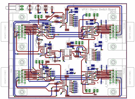
Figure 11: VFX1 Stereo
Switch Board
A custom video board could be designed using the AL128 video processing chips made by Averlogic. This would merge the video switching front end needed for line blanking stereo 3D with the bare minimum needed for the AL128 to operate in VGA->RGB mode. That would be nice and neat, but it’s probably better to just find two used PC/TV Genies and take the boards out of those. Then use them with a video switch board.
The prototype video switcher board together with two PC/TV Genies is shown below in Figure 12. This setup was used to verify correct stereo 3D operation while playing Quake on the VFX1 using a Dell XPS laptop.
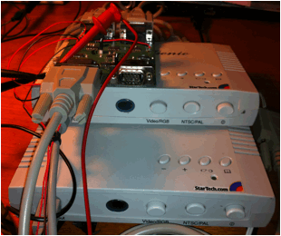
Figure 12: Prototype
Stereo 3D Setup
3. VFX1 Head Tracking and Cyberpuck
3.1 Communication Protocol
3.1.1 ACCESS.bus
The VFX1 uses the ACCESS.bus
protocol to communicate between the VIP card and the HMD for collecting head
tracking data and operating the backlights. ACCESS.bus is also used to communicate with the Cyberpuck.
ACCESS.bus was a pre-USB protocol that was designed on top of the I2C
hardware bus. It was designed to
allow 125 devices to communicate on a single two wire bus. The important thing for us is that
ACCESS.bus uses the I2C bus as its hardware layer.
The reader can refer to the ACCESS.bus protocol pdf in for details of the overall ACCESS.bus scheme. Below the focus will be on the parts of the ACCESS.bus protocol that need to be understood to implement communicate with the VFX1 and Cyberpuck.
Before starting there are a few ACCESS.bus addresses to keep in mind. The default startup address is 0x6E, the linkbox (computer) address is 0x50, the VFX1 address is 0x02, and the Cyberpuck address is 0x04. Initially both the VFX1 and Cyberpuck will be on address 0x6E after power-up. Also, the linkbox can be referred to as the Host, the ACCESS.bus controller, or as the Computer.
VFX1/Cyberpuck ACCESS.bus Configuration Process
There are several steps that must be done in order to establish communication with the VFX1 and Cyberpuck on the ACCESS.bus. These steps are:
1. Power-up/Reset
2. Identification
3. Normal Operation/ Presence Checks
Looking at the ACCESS.bus specification there are multiple other steps and modes of operation but we can simplify here because we know what we’re talking to and we’re only going to talk to a single VFX1 and a single Cyberpuck. Although, the firmware of the linkbox could easily be modified to accept multiple Cyberpucks if desired.
Power-up/Reset
Much of the following is taken verbatim from the ACCESS.bus pdf. At reset or power-up, a device shall always revert to the default address (0x6E) and send an attention message to alert the linkbox of its presence. At system start up or reinitialization, the linkbox shall send a Reset message to all ACCESS.bus addresses in the device address range to insure that all devices on the bus respond at power up. In the firmware code listed in Appendix A, the functions responsible for this step are called accessBUS_reset and accessBUS_serviceAtten.
Identification
The first step in the Identification phase is for the linkbox to send an Identification Request message at the device default address (0x6E). Every device on the bus will then respond with an Identification Reply message. Each device sends its message and received messages are separated based on the identification strings. The linkbox can then assign an address to each device by including the matching identification string in the Assign Address message. A device that receives this message and finds a complete match with the identification string moves its device address to the new assigned value. The device then waits for an “Enable Application Report” message from the host (linkbox). The function in the linkbox firmware that handles this is called accessBUS_assignADDR.
At this point a Capabilities request and reply would come next but we already know the capabilities of our devices so it’s skipped in the linkbox implementation.
Normal Operation/Presence Check
During normal operation the ACCESS.bus manager (linkbox) periodically checks the presense of all devices on the bus. If a device is found missing the bus manager (linkbox) will update the device table. The presence check is simply a NACK or ACK in the I2C messages. The function in the linkbox firmware that handles this is called accessBUS_PC.
At this point we’re ready to stream data from the VFX1 or Cyberpuck by sending an Application Report requesting data. A power management message can also be send to turn on the LCDs of the VFX1. Refer to the linkbox firmware for more details.
3.1.2 Data Stream and Timing
The VFX1 and Cyberpuck run at an I2C clock rate of ~70kHz. The ACCESS.bus protocol states that 100kHz is a maximum. The VFX1 and Cyberpuck will in fact respond and operate on a master clock of 100kHz but still only uses a 70kHz I2C clock.
Both devices are setup to stream their application reports within a 60Hz window. The VFX1 will send out an application report every ~16ms. The Cyberpuck will do the same. Figure 13 below shows timing diagram of the VFX1 and Cyberpuck data streams.
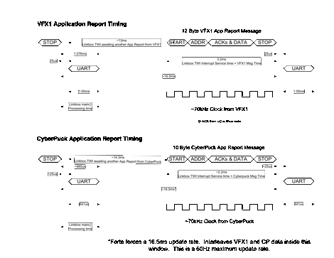
Figure 13: Timing Diagrams
An I2C capture of a VFX1 and Cyberpuck application report is shown below in Figure 14.
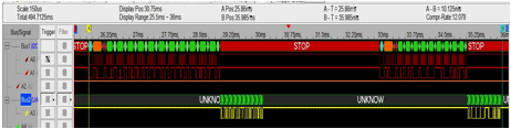
Figure 14: I2C Application Report Capture
The VFX1 outputs an application report containing the following format:
Byte 1 0x50 VIP Card Address: Destination Address
Byte 2 0x02
Source Address/VFX1 address
Byte 3 00001000 Device Data stream, Message length of 8: Protocol Flag
Byte 4 High Byte Sine
Byte 5 Low Byte Sine
Byte 6 High Byte Cosine
Byte 7 Low Byte Cosine
Byte 8 High Byte Pitch
Byte 9 Low Byte Pitch
Byte 10 High Byte Roll
Byte 11 Low Byte Roll
Byte 12 XOR Checksum
The Cyberpuck outputs an Application report that contains the following:
Byte 1 0x50 VIP Card Address: Destination Address
Byte 2 0x04
Source Address/Cyberpuck address
Byte 3 00000110 Device Data stream, Message length of 6: Protocol Flag
Byte 4 Always Zero
Byte 5 Button Status
Byte 6 High Byte Roll
Byte 7 Low Byte Roll
Byte 8 High Byte Pitch
Byte 9 Low Byte Pitch
Byte 10 XOR Checksum
The linkbox firmware as it currently stands strips off the 0x50 byte and sends the rest out the serial port or USB Virtual COM port to be processed by the computer. There’s also a floating point mode in the linkbox firmware that allows all the calculations to be done in firmware and just yaw, pitch, and roll sent to the PC for processing. This will be discussed later in the Tracking linkbox section.
3.2 Sensor Operation
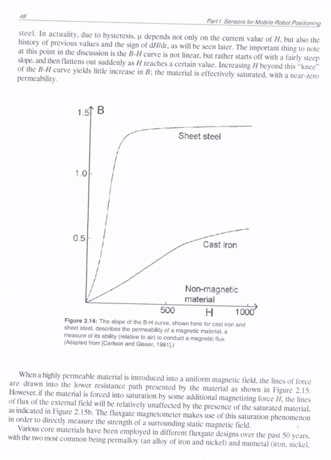
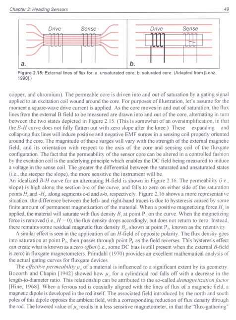
3.2.1 Fluxgate
Rather then re-explain what has been discussed already, below
is a pdf explaining the operation of a fluxgate
magnetometer. The fluxgate is the
sensor used for determining heading in the VFX1.

3.2.2 Electrolytic Tilt Sensor


3.3
Tracking Linkbox
The VFX1 is controlled using a Wiring S board as shown below
in Figure 15. The Wiring S board
contains an Atmega644p running at 16MHz.
It also contains an FTDI FT232R USB to serial chip and an I2C port. This is all that is needed to interface
with the VFX1.
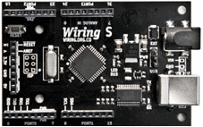
Figure 15: Wiring S Board
The Wiring S board controls the VFX1 LCD power on messages, polls head tracking data, handles serial port communications, performs head tracking floating point calculations, controls the VFX1 power board, controls the stereo switcher board, and controls the PC->TV Genie on-screen adjustments. This board within the VFX1 linkbox is the brains the in chassis.
The VFX1 linkbox tracking firmware provides the following functions through the serial port:
TEST- writes the string “****VFX1 Linkbox****” to the serial port. Used to test communication with the linkbox.
POLL- sets the poll flag in the linkbox for data streaming options. POLL and CONT are the only two options.
CONT- sets the continous flag in the linkbox for data streaming options. POLL and CONT are the only two options.
FLOAT- sets the float flag in the linkbox. Data streamed will be calibrated calculated floating point numbers. No raw data will be streamed. FLOAT or INT are the only two options.
INT- data polled will be raw data. FLOAT or INT are the only two options.
P_VF- prints out a set of VFX1 head tracking data if the POLL command was sent. Takes into consideration the FLOAT or INT commands.
P_CP- prints out a set of Cyberpuck data if the POLL command was sent. Takes into consideration the FLOAT or INT commands.
AB_RST- issues an ACCESS.bus reset to all devices on the bus. VFX1 and Cyberpuck should be the only two devices on the bus.
APP_ON_VF- issues the application report ON command to the VFX1 is the VFX1 is present on the ACCESS.bus.
APP_OFF_VF- issues the application report OFF command to the VFX1 if the VFX1 is present on the ACCESS.bus.
APP_ON_CP- issues the application report ON command to the Cyberpuck if the Cyberpuck is present on the ACCESS.bus.
APP_OFF_CP- issues the application report OFF command to the Cyberpuck if the Cyberpuck is present on the ACCESS.bus.
LCD_ON- turns the VFX1 LCDs ON if the VFX1 is present on the ACCESS.bus.
LCD_OFF- turns the VFX1 LCDs OFF if the VFX1 is present on the ACCESS.bus.
WR_EE_AAAA_DD- writes EEPROM location AAAA with data DD.
RD_EE_XXXX- reads EEPROM location XXXX.
R_INC- activates the right PC->TV Genie on-screen up button.
R_DEC- activates the right PC->TV Genie on-screen down button.
R_SEL- activates the right PC->TV Genie on-screen select button.
R_MAN- activates the right PC->TV Genie on-screen menu.
L_INC- activates the left PC->TV Genie on-screen up button.
L_DEC- activates the left PC->TV Genie on-screen down button.
L_SEL- activates the left PC->TV Genie on-screen select button.
L_MAN- activates the left PC->TV Genie on-screen menu.
STEREO_X- 0 selects non-stereo mode. 1 selects line-blanking stereo mode.
VIDEO_X- 0 selects the left channel only for the input. 1 selects dual channel with both left and right input video ports being active.
HMD_ON- turns the VFX1 ON. Applies 5V to the VFX1 supplies.
HMD_OFF-turns the VFX1 OFF. Turns off the 5V supplies to the VFX1.
4. Full Linkbox Solution
A full system is shown below in Figure 16. The VFX1 linkbox is shown in the middle and contains the two PC->TV Genies, the video switcher for stereo 3D, a Wiring S board containing an Atmega644pa, and a power board for supplying power to the VFX1. All the boards are controlled by the Atmega644pa.
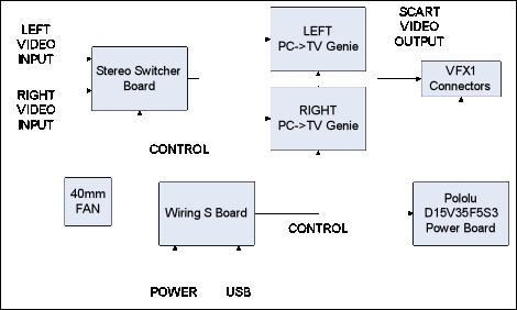
Figure 16: Linkbox Block Diagram
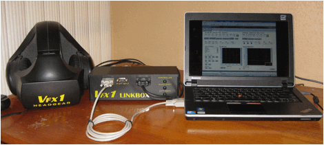
Figure 17: Full Linkbox
Solution
On the front side of the linkbox are the Left/Right inputs for the stereo switcher board and the VFX1 output connector. A close up of the VFX1 linkbox chassis front panel is shown below in Figure 18.
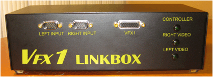
Figure 18: VFX1 Linkbox
Front Panel
The rear panel consists of the stereo switcher board outputs, the PC->TV Genie inputs and monitor pass-thrus, the Wiring S USB and power connections, microphone output, and audio input. A close up of the rear panel is shown below in Figure 19.
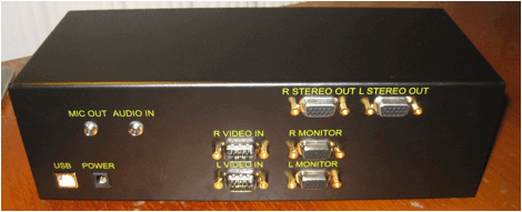
Figure 19: VFX1 Linkbox
Rear Panel
The sides of the linkbox consist of a fan on one end and a vent on the other. This is to pull air across the PC->TV genie boards for cooling.
This full linkbox solution provides video to the VFX1, stereo 3D in interlaced mode, and polls tracking data from the VFX1 head tracking sensors. Through the control software various modes of operation can be entered for both video and tracking data. Video can be put in dual input mode, stereo 3D interlaced mode, or regular video. Monitor ports are also provided to display video externally while using the VFX1. Tracking data can be polled from the VFX1 head tracker and Cyberpuck in raw data format or in calibrated floating point format. All PC->TV Genie functions are controlled through the linkbox as well.
5. Calibration Suite
The Calibration Suite or CalSuite
is a LabWindows based GUI written to calibrate the
VFX1 and Cyberpuck sensors, control the linkbox, display calculated sensor data, and map sensor
data to mouse movements. A screen
shot of the CalSuite GUI is shown below in Figure 20.
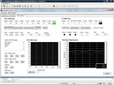
Figure 20: CalSuite
GUI
There are several tabs in the CalSuite
software: Calibration, Cal Table, and VFX1 Linkbox.
The Calibration tab displays captured sensor data and plots
it to the screen. An example of
the Roll sensor response of the VFX1 headset is shown below in Figure 21.
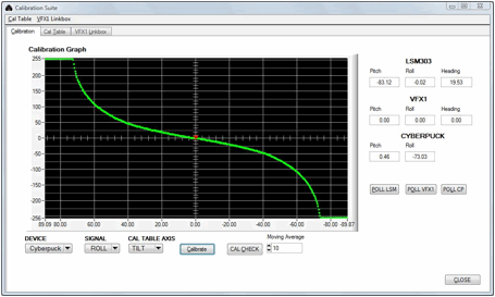
Figure 21: Roll Sensor Calibration
Curve
When the roll sensor has been calibrated, a cal check can be performed. Below in Figure 22 is the calibrated roll sensor response.
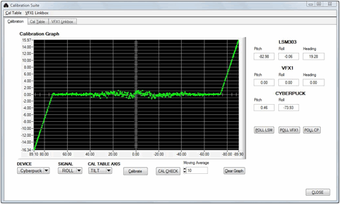
Figure 22: Roll Cal Check Response
Curve
The Cal Table tab is shown below in Figure 23. This tab provides calibration functions
for the LSM303 reference sensor that is attached to the calibration tilt table
discussed below in Section 5.1.
This sensor is what the VFX1 sensors are calibrated against during tilt
and pan measurements.
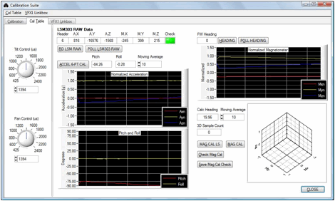
Figure 23: Cal Table Tab
The VFX1 Linkbox tab of the Cal Suite controls the various functions of the VFX1 and Cyberpuck. It also contains the video control buttons for the PC->TV genies. Mouse mapping functions are also controlled on this tab.
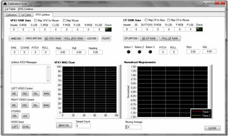
Figure 24: VFX1 Linkbox
Tab
5.1 Calibration Tilt Table
The calibration tilt table consists of a custom designed
controller board (atmega644pa), LSM303DLH breakout board from Pololu, two PRT-10804 power supply boards from SparkFun, a ServoCity DDT560H
Direct Drive Tilt Mount, HS-985MG servos operating at 180 degrees, and a ServoCity SPG400A-BM-360 Servo power gear box. The image of the system is shown below
in Figure 25. My first
“calibration table” was a piece of plywood with degree markings. It has come a long way.
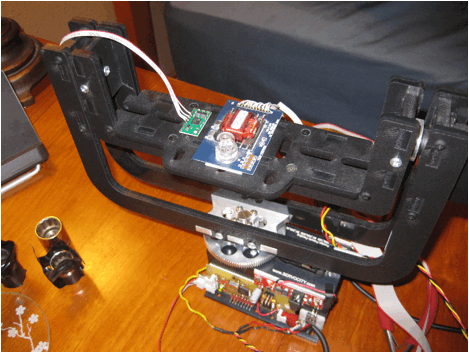
Figure 25: Calibration Table
The entire system is computer controlled using the cal suite software. Sub degree tilt movements are possible along with pan movement for yaw measurements of the VFX1 head tracker.
5.2 Electrolytic Tilt Sensor Calibration
This calibration is relatively straight forward. The output needs to be plotted and a
calibration curve generated. The
electrolytic tilt sensors output a tangent like curve, as described previously,
in response to tilt. However, like
most sensors these output curves are not ideal over our entire +/-70 degree
tilt range. To compensate for
this, the sensor output is characterized and then a piece-wise calibration
curve is used to correct it. The
calibration table is set to tilt in 1 degree increments and the output response
is plotted. This data is then
imported into Excel and a piece-wise trend line is created. I’ve chosen to do a 5 part correction
curve. These equations are then
entered into the CalSuite software and the VFX1 Linkbox firmware to provide corrected tilt output. The same procedure is repeated for both
the pitch and roll axes of both the VFX1 and the Cyberpuck. An example curve for VFX1 pitch is
shown below in Figure 26.
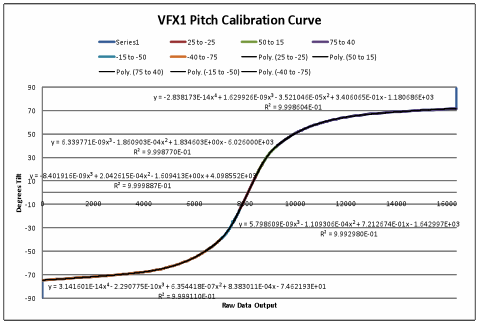
Figure 26: VFX1 Pitch Calibration Correction Curve
This procedure needs to be repeated 4 times: pitch and roll
for the VFX1, pitch and roll for the Cyberpuck. Without a calibration table this
process can be extremely tedious and error prone. Trust me, I’ve done it.
5.3 Fluxgate
Calibration
The fluxgate calibration is more complicated. This sensor needs hard-iron and
soft-iron corrections, sensitivity adjustments, and normalization. This is just to get good data from the
sensors, not taking into account the efforts needed to generate a tilt
compensated heading.
The calibration table here is used to verify the
calibration. Taking the actual
data requires the user to rotate the VFX1 in a sphere over several
iterations. It’s a trial and error
process because the data can be noisy and a spike in the data will cause
erroneous cal coefficients to be generated. When it’s all said and gone the fluxgate sensor should give
you an output that is normalized to +/-1 in the shape of a 3D sphere centered on
the origin of a Cartesian plot.
There should be no offsets and it should not be elliptical.
Rather than repeat what’s already been done, please refer to
“Applications of Magnetic Sensors for Low Cost Compass Systems” by Michael J.
Caruso of Honeywell, SSEC. An
excellent application note that was used to implement most of the accelerometer
and magnetometer calibrations of both the LSM303 and VFX1 fluxgate sensor is
“AN3192: Using LSM303DLH for a tilt compensated electronic compass” by STMicro. You
can also refer to the CalSuite C files for the actual
source code implemented.
As you follow the Honeywell and STMicro
PDFs, along the way you should get data from the VFX1 as shown in the Figures
below.
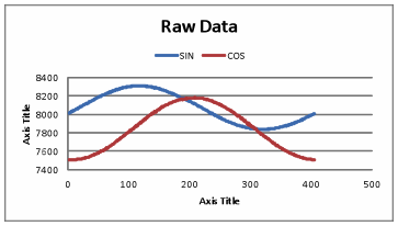
Figure 27: Raw Xh
Yh VFX1 Fluxgate Data
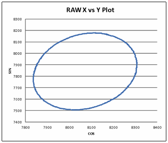
Figure 28: X-Y Plot of VFX1 Xh Yh data
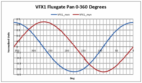
Figure 29: Pan Rotation on Calibration Table
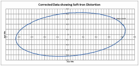
Figure 30: Example of Soft-Iron Distortion
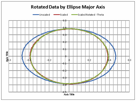
Figure 31: Soft-Iron Correction Plots mentioned in ST Micro PDF
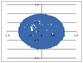
Figure 32: Corrected Mag Check data of VFX1 Fluxgate from CalSuite
Software
5.4 Generating
a Heading
This is where the magic happens. You can refer to the STMicro doc
and Honeywell doc referenced above for the overall method. However, you need US Patent #5,373,857
for the VFX1 fluxgate equation.
This patent is for a “Head Tracking Apparatus” by inventors Paul J.
Travers and Ying S. Yee of Forte Technologies. This is the only document I won’t include in the zip file
where this word document was found.
Legally I’m not sure I can include it so it’s been omitted. However, you can
pay and download it via the United States Patent Office. You may also be able to get it free via
Goggle Patents.
The Forte patent gives the
equation V=M2cosθcosφ + M1sinφ. “The earth’s magnetic field has a
vertical component M1 and horizontal component M2. If the azimuth sensor is oriented with its access making an
angle θ in the horizontal and a tilt angle φ, then the output voltage
V is described by V=M2cosθcosφ + M1sinφ”
(US Patent 5,373,857).
Using this equation you can
generate what the fluxgate output should look like at various headings
depending on tilt. Shown below are
some theoretical calculations.
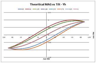
Figure 33: Theoretical Fluxgate Curves at various tilts and headings
Now using the calibration table and fixing the heading and
then adjusting the tilt, the measured response of the VFX1 fluxgate sensor output
is shown below in Figure 34.
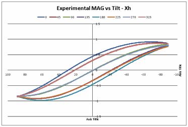
Figure 34: Experimentally Measured Fluxgate Tilt Response
As can be seen above, the experimental data of Figure 34
matches very well with the theoretical data of Figure 33. This shows the equation in the Forte
Patent can be used to achieve tilt compensated heading from the VFX1 head
tracker.
That was quite a quick pass through what took a very long
time to decipher. Please refer to
the zip file that this document came in for more information on how this is all
put together. Also, the CalSuite C files show exactly how all of this was
implemented.
I can’t stress enough how CRITICAL it is that your
calibrations are accurate to get a good tilt compensated heading from the VFX1
head tracker. Multiple refinements
and iterations led me to get a typical +/-2 degree agreement between the VFX1
and my reference LSM303 sensor.
However there are still places as you’ll see below where the error is
larger than 2 degrees. With rough
sensor calibrations you can have errors of up to 10-20 degrees. SO BE WARNED.
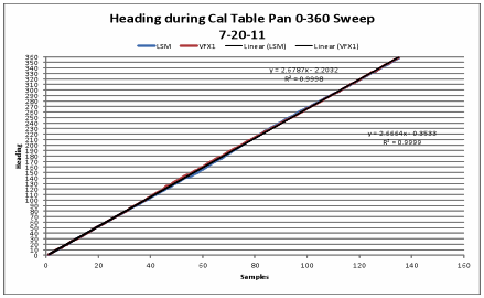
Figure 35: LSM303 vs
VFX1 Heading
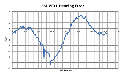
Figure 36: LSM303 vs
VFX1 Heading Error
5.5 Mouse Code
Please refer to the CalSuite C files for actual source code implementation.
![]()
